
Semiconductors sit at the centre of modern industry. India’s ambition to build domestic capability in this sector is not a vanity project. It is a strategic necessity. Four years after the launch of the ₹76,000 crore India Semiconductor Mission (ISM), the government has moved to the next phase. ISM 2.0, announced in the Union Budget 2026–27, is meant to shift the programme from attracting fabs and packaging plants to building equipment, materials, design intellectual property and supply-chain depth.
The shift is overdue. Semiconductor ecosystems are not built by one subsidy window or a five-year policy cycle. They require patient capital, technology transfer, trained engineers, assured infrastructure and a dense supplier base. India can assemble phones at scale within a decade. It cannot build a competitive chip ecosystem in the same manner.
READ | India Semiconductor Mission enters the production phase
India Semiconductor Mission
The first phase of ISM sought to bring anchor investments into fabrication and packaging. The results are not comparable with Taiwan, South Korea or China. But that is the wrong benchmark for a country that had almost no commercial semiconductor manufacturing base.
The government says 10 projects with investment commitments of about ₹1.6 lakh crore had been approved by early 2026. Subsequent approvals have taken the number to 12, including Crystal Matrix’s compound semiconductor and display-related facility in Dholera and Suchi Semicon’s OSAT facility in Surat. The larger projects include Micron’s ₹22,516 crore ATMP facility in Sanand and the Tata Electronics–Powerchip Semiconductor Manufacturing Corporation fab in Dholera, estimated at about ₹91,000 crore with planned capacity of 50,000 wafers a month.
These are important beginnings. They are not yet an ecosystem.
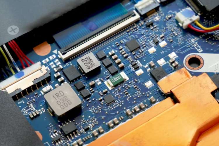
A fab does not work in isolation. It needs specialty gases, chemicals, wafers, masks, process tools, advanced packaging materials, reliable power, ultra-pure water, clean-room systems, precision logistics and highly trained workers. India has parts of this chain. It does not yet have the depth, reliability or clustering that make East Asian semiconductor hubs formidable.
ISM 2.0 must build supply chains, not just plants
This is why ISM 2.0 matters. The government’s own description of the new phase stresses equipment and materials, full-stack Indian IP and stronger domestic and global supply chains. The emphasis is right. India’s semiconductor problem is not only the absence of fabs. It is the thinness of the industrial base around them.
ISM 2.0 should not be judged merely by the size of its subsidy envelope. Its stated focus is equipment, materials, design IP, talent and supply-chain depth. That is where India’s semiconductor weakness lies. The first phase needed generous incentives to attract anchor investors. The next phase must reduce dependence on imported tools, process inputs and foreign-controlled know-how.
There are reports that the next phase may reduce direct capital subsidies for some fabrication and packaging projects from the current 50% level and direct more support towards ecosystem gaps. That would be a sound correction if implemented with discipline. The first phase needed generous incentives to pull in anchor investors. The second phase must make those investments less dependent on imports and foreign process control.
Indian MSMEs will not become globally competitive suppliers of semiconductor inputs in five years. The sector rewards precision, repeatability and certification. These are not acquired by notification. They come from long contracts, technical handholding, common facilities, metrology labs and integration with large manufacturers. ISM 2.0 should be judged by how many such suppliers it creates, not merely by the number of project approvals it announces.
Taiwan, South Korea, Japan, China and the United States did not build their semiconductor positions through market forces alone. Their ecosystems were shaped by state support, procurement, research institutions, industrial finance and close coordination with private firms. India need not copy any one model. But it cannot avoid the lesson that semiconductor capability is cumulative.
READ | Budget 2026: Semiconductors drive MeitY’s recalibrated tech spend
Semiconductor supply chains are now geopolitics
The global context strengthens India’s case. Chips are now central to economic security and military capability. The US-China technology conflict, export controls on advanced chips and curbs on semiconductor equipment have made supply-chain concentration a political risk. Multinational firms want alternatives. India wants to be one of them.
India has some advantages. It has a large electronics market, a growing manufacturing base, policy continuity and strategic partnerships with the United States, Japan and Taiwan. It also has an established chip design base. Global firms such as Intel, Qualcomm, NVIDIA and Texas Instruments have long operated design and R&D centres in Bengaluru, Hyderabad and Noida. India’s engineering talent is a real asset, especially in chip design, embedded systems and electronic design automation.
But design strength does not automatically translate into manufacturing strength. The two must be connected through productisation, prototyping, testing and commercial scale. That is where policy needs sharper execution.
The Design Linked Incentive scheme and the Chip to Startup programme are useful, but they must produce firms that own usable IP and sell into real markets. The DLI scheme offers financial incentives and design infrastructure support for integrated circuits, chipsets, systems-on-chip, systems and IP cores over five years. This is encouraging. It is not yet industrial capability.
Design capability will not mature without a route to market. The government can help by using defence, telecom, railways, power equipment and public digital infrastructure as early demand anchors for trusted chips designed or packaged in India. Procurement standards, testing labs and assured pilot orders can do what subsidies alone cannot: convert design talent into commercial products.
Electronics manufacturing gives India a base
India’s electronics success offers one lesson and one warning. The production-linked incentive scheme helped India attract smartphone assembly at scale. Government data show that electronics production has expanded sharply over the past decade, while mobile phone exports have also risen.
This proves that incentives, scale and market access can shift manufacturing. It also shows the limit of assembly-led success. Value addition remains constrained when components, tools and materials are imported. Semiconductors are the next test of whether India can move from assembly to industrial depth.
India should pick the right semiconductor battles
India should not begin by trying to match Taiwan or South Korea in cutting-edge logic chips. Leading-edge fabs cost enormous sums, depend on tightly controlled technologies and face fast product cycles. Access to advanced lithography and process equipment is dominated by a few global firms such as ASML, Applied Materials and Tokyo Electron. Export controls can quickly alter what is commercially possible.
READ | Global semiconductor alliance exposes India’s tech vulnerability
India’s more practical opportunity lies in mature-node manufacturing, compound semiconductors, sensors, power electronics, OSAT services and advanced packaging. These segments matter for electric vehicles, telecom, industrial systems, defence, renewable energy and consumer appliances. They also fit better with India’s current industrial capabilities.
The harder question is not whether India can attract plants, but whether it can create reliable demand for their output. Semiconductor projects need long-term customers, not just subsidy approval. Mature-node chips, power devices, sensors and packaging services will become viable only if Indian automobile, telecom, defence, renewable energy and consumer electronics firms commit volumes through predictable procurement. Without such demand aggregation, fabs and OSAT units may remain subsidy-backed assets rather than competitive nodes in a global supply chain.
Infrastructure remains the other constraint. Semiconductor plants need uninterrupted power, ultra-pure water, stable logistics and disciplined industrial services. Even minor disruptions can destroy output and raise costs. Gujarat, Tamil Nadu, Karnataka, Uttar Pradesh, Odisha and Assam are competing for projects. Competition among states is useful. But semiconductor clusters require standards that go beyond land allotment and state subsidies.
Global competition will only intensify. The United States has the CHIPS and Science Act. The European Union has the European Chips Act. China continues to pour state capital into its semiconductor industry despite Western restrictions. TSMC now expects the global semiconductor market to exceed $1.5 trillion by 2030, driven by artificial intelligence and high-performance computing.
India cannot win this race by announcing ambitions. It can compete only by choosing segments carefully, funding them consistently and measuring progress honestly. ISM 2.0 is useful because it recognises that semiconductors are an ecosystem, not a trophy investment. Its success will depend on whether India can build the unglamorous parts of that ecosystem: suppliers, tools, materials, process discipline and skilled technicians.
The country has made a start. The harder work begins now.